PDN and decoupling: target impedance and the capacitor network
Power distribution network, target impedance Zt = ΔV/ΔI, the role of bulk and HF capacitors, anti-resonance and how to choose values to keep the rail impedance low.
A fast digital circuit does not draw current steadily: it switches it at every clock edge. The job of the power network is to supply those current spikes without making the rail voltage swing. This tool sizes the capacitor network that makes it possible; this page explains the model.
The power distribution network
The power distribution network (PDN) is everything between the regulator and the chip’s power pins: the PCB copper planes, the vias, the traces and the decoupling capacitors. Seen from the load it is not an ideal short but an impedance Z(f) that changes with frequency, because every element has parasitic resistance, inductance and capacitance.
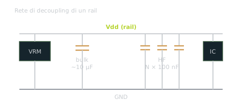
The consequence is direct: every current step ΔI the load demands develops across that impedance and produces a voltage change on the rail.
That ΔV is the power-supply noise. Keeping it within the chip’s limits means one thing: keeping Z(f) low across the whole band over which the load switches.
Target impedance
The classic design criterion turns the noise requirement into an impedance threshold. You fix the maximum allowed ripple ΔV on the rail and the transient switching current ΔI; their ratio is the target impedance:
The PDN meets the target if its impedance stays below Zt across the whole band of interest. The tighter the ripple (low-voltage cores, ADCs, PLLs) or the larger the peak current, the lower Zt — which for modern cores easily drops into the milliohm range. A 1 V rail with 50 mV ripple and a 5 A transient calls for a Zt of 10 mΩ.
Decoupling: bulk and HF
Decoupling places capacitors close to the load so they supply the transient current locally, before it has to come from the regulator through the inductance of the planes. But no capacitor is ideal: beyond its capacitance C it has a series resistance (ESR) and, above all, a parasitic series inductance (ESL). The impedance of a real capacitor is
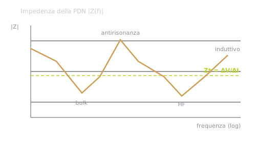
at low frequency the capacitive term 1/(ωC) dominates and falls with f; above the self-resonant frequency ωL dominates and the impedance rises again. A single capacitor is therefore low-impedance only over a narrow band. To cover several decades a two-tier network is used:
- Bulk — large capacitance (µF), covering the low frequencies where a lot of charge is needed. It is sized so its capacitive reactance stays below Zt at a low frequency (here a decade below fmax):
- HF bank — many small capacitors (e.g. 100 nF) in parallel. At high frequencies the bank impedance is ESL-dominated, and putting N caps in parallel divides the effective ESL by N. The design condition is that the residual inductive reactance at fmax stays below Zt:
Hence two intuitive rules: tighter Zt or higher fmax call for more HF capacitors in parallel. N grows quickly, and it is the first sign that a target is severe — how quickly is worth seeing:
| ΔV | ΔI | Zₜ | f max | HF capacitor count |
|---|---|---|---|---|
| 100 mV | 2 A | 50.00 mΩ | 20 MHz | 3 |
| 50 mV | 5 A | 10.00 mΩ | 20 MHz | 13 |
| 50 mV | 5 A | 10.00 mΩ | 100 MHz | 63 |
| 30 mV | 10 A | 3.00 mΩ | 50 MHz | 105 |
| 50 mV | 20 A | 2.50 mΩ | 100 MHz | 252 |
| 20 mV | 30 A | 0.67 mΩ | 100 MHz | 943 |
| 10 mV | 50 A | 0.20 mΩ | 200 MHz | 6284 |
The bold rows are the point. The formula has no ceiling at all: ask for 0.2 mΩ up to 200 MHz and it answers 6284 capacitors, with the same straight face it uses to propose three. A number like that is not a bill of materials: it is the model saying “this target is not reachable this way” without having the vocabulary to say it.
The shared-inductance wall
The reason is in the ESL/N assumption. Dividing by N holds if every capacitor has its own path to the load. In reality part of the inductance is shared — the run inside the package, the pin, the via down to the die, the loop in the planes near the load — and that does not divide at all:
The right-hand side is the ceiling: the highest frequency at which that target is reachable, whatever N is.
| Zₜ | shared L 0.2 nH | 0.5 nH | 1 nH | 2 nH |
|---|---|---|---|---|
| 1 mΩ | 0.80 MHz | 0.32 MHz | 0.16 MHz | 0.08 MHz |
| 5 mΩ | 3.98 MHz | 1.59 MHz | 0.80 MHz | 0.40 MHz |
| 10 mΩ | 7.96 MHz | 3.18 MHz | 1.59 MHz | 0.80 MHz |
| 50 mΩ | 39.8 MHz | 15.9 MHz | 7.96 MHz | 3.98 MHz |
| 100 mΩ | 79.6 MHz | 31.8 MHz | 15.9 MHz | 7.96 MHz |
| 500 mΩ | 398 MHz | 159 MHz | 79.6 MHz | 39.8 MHz |
A 10 mΩ target with 0.5 nH shared holds up to 3.2 MHz, not 100. And the effect on the parallel bank is immediate: with 0.3 nH shared, going from 1 to 128 capacitors at 100 MHz gains 4.22 times, not 128.
| N | ESL/N | + 0.3 nH shared | |Z| at 100 MHz | Gain over N = 1 |
|---|---|---|---|---|
| 1 | 1000 pH | 1300 pH | 0.817 Ω | × 1.00 |
| 2 | 500 pH | 800 pH | 0.503 Ω | × 1.63 |
| 4 | 250 pH | 550 pH | 0.346 Ω | × 2.36 |
| 8 | 125 pH | 425 pH | 0.267 Ω | × 3.06 |
| 16 | 63 pH | 363 pH | 0.228 Ω | × 3.59 |
| 32 | 31 pH | 331 pH | 0.208 Ω | × 3.92 |
| 64 | 16 pH | 316 pH | 0.198 Ω | × 4.12 |
| 128 | 8 pH | 308 pH | 0.193 Ω | × 4.22 |
The knee sits where ESL/N equals L_shared, that is at N ≈ ESL/L_shared: three or four capacitors for a mediocre layout, about ten for a good one. At that point |Z| is twice its asymptotic floor, so everything added afterwards — be it a thousand capacitors — cannot be worth more than a factor of 2 in total. That is the practical answer to “how many capacitors do I fit?”: up to the knee every cap pays, past it you are buying one halving and nothing else, at the price of area, cost and vias.
And when the target sits below the ceiling, no number of capacitors will fix it: you have to lower L_shared (shorter and more numerous vias, thinner dielectric between the planes, caps on the component side) or move the capacitance closer — onto the package or the die, where the connection inductance is orders of magnitude smaller. That is why modern SoCs carry integrated capacitance: above a few tens of MHz, PCB decoupling has stopped being in the game.
Anti-resonance
Combining bulk and HF has a side effect. Between a capacitor with large C and higher ESL (the bulk) and one with small C (the HF bank) a parallel-series resonance forms: at an intermediate frequency the bulk inductance and the HF bank capacitance resonate and the PDN impedance shows a peak — the anti-resonance — right in the band where we want it low.
An indicative estimate of where it appears:
with L_bulk the ESL of the bulk capacitor and C_HF,tot the total HF bank capacitance. It is an order of magnitude to know where to look, not a simulation value: the formula gives the peak’s frequency and says nothing about its height, which is the thing that decides whether the design passes.
How high the peak is: ESR is the only thing that matters
The height comes from computing the impedance of the two RLC branches in parallel. On a reference network — a 10 µF bulk with 2 nH, a bank of 20 × 100 nF with 1 nH each — the peak depends almost only on the ESR:
| Bulk ESR | Single HF ESR | Anti-resonance peak |
|---|---|---|
| 2 mΩ | 2 mΩ | 384.3 mΩ @ 2.72 MHz |
| 5 mΩ | 5 mΩ | 155.7 mΩ @ 2.73 MHz |
| 10 mΩ | 10 mΩ | 81.3 mΩ @ 2.73 MHz |
| 50 mΩ | 20 mΩ | no peak: |Z| monotonic |
| 200 mΩ | 50 mΩ | no peak: |Z| monotonic |
| 1000 mΩ | 100 mΩ | no peak: |Z| monotonic |
The peak goes as 1/ESR: halving the ESR doubles it. And the last three rows are the surprising result: above 50 mΩ there is no peak at all, |Z| becomes monotonic and the anti-resonance is damped away. The conclusion goes against every designer’s instinct: a “better” capacitor, because of its lower ESR, makes the PDN worse exactly where it is weakest. ESR is not a defect to minimize, it is the network’s damping — which is why a few milliohms of series resistance are sometimes added on purpose, or a lossier dielectric deliberately chosen.
Spreading the values: it does not work the way it is told
The classic advice is to spread the bank over several values to “fill the hole”. Computed on the same network, at equal ESR (5 mΩ per capacitor), it goes like this:
| Bank composition | Peaks | The worst one |
|---|---|---|
| 20 × 100 nF | 1 | 155.7 mΩ @ 2.73 MHz |
| 10 × 1 µF + 10 × 100 nF | 2 | 36.2 mΩ @ 11.87 MHz |
| 7 × 1 µF + 7 × 100 nF + 6 × 10 nF | 3 | 249.9 mΩ @ 42.80 MHz |
From one value to two the worst peak drops by 4.3 times and moves up in frequency: the advice works. From two to three it goes back up, and at 250 mΩ it is worse than the starting point. The reason is that every added value brings its own anti-resonance against the inductance of the bank below it — the number of peaks grows with the number of distinct values — and the 10 nF caps resonate at 42.8 MHz, where there is no longer enough copper nor enough ESR to damp anything.
So the correct rule is tighter: two decades of capacitance, each with enough capacitors to damp its own resonance, beat three decades spread thin. And adding a decade only makes sense if that band is genuinely needed, because a capacitor is only useful above its own self-resonance:
| Capacitance | Typical ESL | Self-resonance |
|---|---|---|
| 10 µF | 2.0 nH | 1.13 MHz |
| 1 µF | 1.2 nH | 4.59 MHz |
| 100 nF | 1.0 nH | 15.92 MHz |
| 10 nF | 0.8 nH | 56.27 MHz |
| 1 nF | 0.6 nH | 205.47 MHz |
A 10 nF part starts working at 56 MHz: fitting it on a network that only has to reach 20 MHz adds a peak and no benefit.
Choosing the values
The values the tool suggests are rounded to the E12 series, the most common and lowest-cost. The model uses a fixed ESL (1 nH for the HF cap, 2 nH for the bulk), typical for small packages with dedicated vias. They are a starting point to verify in a real PDN simulation before layout, because:
- the effective ESL depends strongly on the layout (via length, loop area, position relative to the pin);
- the PCB has its own distributed plane capacitance that joins the network at high frequencies;
- at very low targets (below the milliohm) decoupling alone is not enough: you have to work on the power planes and the PCB’s power/ground coupling.
Limits
- Fixed-ESL model: no dependence on the real package, layout or temperature; ESR neglected in the sizing.
- No PCB plane capacitance and no plane/via impedance.
- The anti-resonance is a single-degree-of-freedom estimate, not the full impedance spectrum of the network.
- Demonstrative tool, not a SPICE solver nor a PDN simulator.
References
- Power-integrity and signal-integrity literature on PDN sizing, target impedance and the anti-resonance of capacitor banks — the reference for the method and the limits of the fixed-ESL model.
- Capacitor manufacturers’ application notes on ESR/ESL, self-resonant frequency and mounting inductance.
- Related tool — the PDN / Decoupling Planner puts this page into practice: enter rail, transient and fmax and get Zt, bulk, HF bank and the indicative anti-resonance frequency.
A similar project?
Acoustics, embedded, calculation tools: if you have a related use case, let’s talk.