PDN Decoupling Planner
Size the decoupling network of a power rail: from the target impedance Zt = ΔV/ΔI it derives the bulk capacitance and the number of parallel HF capacitors needed to keep the impedance below target up to fmax, and estimates where the anti-resonance peak may appear. Demonstrative tool.
PDN / decoupling planner tool
1 · Rail and transient
Engineering estimates, not a SPICE solver. Fixed ESL: 1 nH per HF cap, 2 nH for the bulk. The HF cap count follows the inductive limit N ≥ 2π·fmax·ESL/Zt; the bulk follows the capacitive reactance at fmax/10.
Suggested network
How it works
What is a PDN?
The power distribution network (PDN) is everything that carries current from the regulator to the chip’s power pins: copper planes, vias, traces and decoupling capacitors. Seen from the load it is an impedance Z(f) that varies with frequency; on each current step ΔI it develops ΔV = Z·ΔI, the rail noise. Decoupling means keeping Z low across the band.
What is the target impedance?
The classic criterion sets a threshold: the PDN impedance must stay below a target impedance Zt, equal to the allowed ripple divided by the transient switching current — Zt = ΔV/ΔI. The tighter the allowed ripple or the larger the peak current, the lower the Zt to hold, which easily ends up in the milliohm range.
The classic design criterion sets a threshold: the PDN impedance must stay below a target impedance Zt equal to the allowed ripple divided by the transient switching current.
The tighter the allowed ripple (cleaner rails, low-voltage cores) or the larger the peak current, the lower the Zt to hold — and Zt easily ends up in the milliohm range.
Why are bulk and HF capacitors needed?
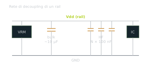
No capacitor is ideal: beyond its capacitance it has a parasitic series inductance (ESL) and above its resonance it behaves like an inductor. So a two-tier network is used: the bulk (µF) covers the low frequencies, where 1/(ωC) must stay below Zt; a bank of N parallel HF caps (nF) divides the ESL by N, keeping the impedance below Zt up to fmax.
No capacitor is ideal: beyond its capacitance it has a parasitic series inductance (ESL). Above its own resonant frequency a cap behaves like an inductor and its impedance starts rising again as ωL. This is why a two-tier network is used:
- Bulk — large capacitance (µF) covering the low frequencies, where the capacitive reactance 1/(ωC) must stay below Zt. Larger package, higher ESL: effective only until it resonates.
- HF bank — many small capacitors (nF) in parallel. At high frequencies the bank impedance is ESL-dominated: putting N caps in parallel divides the effective ESL by N (ESL/N), bringing ωL below Zt.
The design condition on the HF bank is that the residual inductive reactance at fmax stays below Zt:
The bulk is sized instead so its capacitive reactance stays below Zt at a low frequency (here a decade below fmax), then rounded to the nearest E-series value:
What is anti-resonance?
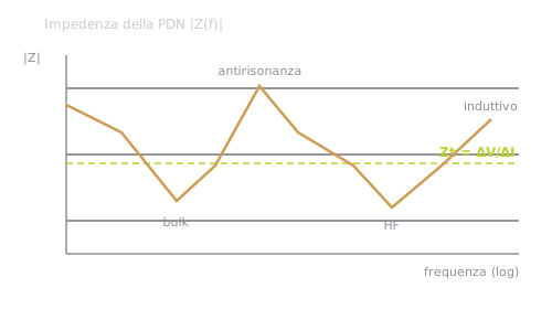
Between the bulk (large C, higher ESL) and the HF bank (small C) a parallel-series resonance forms: at an intermediate frequency the impedance shows a peak — the anti-resonance — right where we want it low. It is the main risk of a multi-capacitor network; the point is estimated by f ≈ 1/(2π√(L_bulk·C_HF,tot)) and damped by choosing intermediate values or controlling the ESR.
Between the bulk (large C, higher ESL) and the HF bank (small C) a parallel-series resonance forms: at an intermediate frequency the bulk inductance and the HF bank capacitance resonate and the PDN impedance shows a peak — the anti-resonance — right where we want it low. It is the main risk of a multi-capacitor network. An indicative estimate of the point:
with L_bulk the bulk ESL and C_HF,tot the total HF bank capacitance. It is an order of magnitude to know WHERE to look, not a simulation value: the peak is damped by choosing intermediate values, controlling the ESR or spreading the bank over several values.
Choosing the values
The suggested values are rounded to the E12 series, the most common and lowest-cost. They are a starting point to verify in a PDN simulation (model with real ESL/ESR, PCB plane capacitance, load spread spectrum) before layout: very low targets (below the milliohm) leave the domain of decoupling alone and call for power planes and the PCB's distributed capacitance.
Fixed-ESL model, no SPICE solver — see the limits in the wiki.