PCB trace width and controlled impedance
Sizing the traces of a printed circuit board: width for current capacity (IPC-2221), resistance and voltage drop; the characteristic impedance of microstrip and stripline and why it matters for signal integrity.
A PCB trace does two jobs that are designed separately: carrying current without overheating, and — at high frequencies — propagating a signal without reflecting it. The tool covers both: current sizing with the IPC-2221 curve and the controlled impedance of microstrip and stripline. This page explains the two physics.
Width for current capacity: the IPC-2221 curve
A current-carrying trace dissipates by Joule effect and heats up. The generic IPC-2221 standard (heir of IPC-D-275) captures in an empirical curve the relation between the DC current I, the allowed temperature rise ΔT above ambient and the copper cross-section area. Inverting it gives the minimum area; dividing by the copper thickness, the width:
The constant k depends on the layer: k = 0.048 for external traces, air-cooled, and k = 0.024 for internal ones, which dissipate worse. Mind the factor: halving k does not double the width, because the exponent is 1/0.725. The exact ratio is 21/0.725 ≈ 2.601. Copper thickness is measured in ounces: 1 oz ≈ 35 µm ≈ 1.378 mil. More copper means a narrower trace for the same capacity, the usual lever when space is tight (2 oz copper on power boards).
A worked example
For 1 A with ΔT = 10 °C on 1 oz copper, an external trace needs an area of ~16.3 mil² and therefore a width of ~11.8 mil (0.30 mm). The same current on an internal layer (half the k) needs ~42.4 mil², i.e. ~30.8 mil (0.78 mm): 2.6 times, not double. This is the calculation that separates a signal trace from a power one.
Why the internal trace costs 2.6 times, and why it may not
The model’s k coefficient distinguishes only two cases: 0.048 for an external trace and 0.024 for an internal one. That factor of two weighs more than two, because the exponent amplifies it: halving k multiplies the width by 2^1.379 = 2.601. A 2 A trace that asks for 20.2 mil on an outer layer asks for 52.5 mil buried.
The reasoning behind the halved k is that a buried trace has no air cooling it. And this is where the model shows its age: the IPC-2221 curves have one geometric variable (the cross-section area) and one bit of context (internal or external). They know nothing about the laminate’s thermal conductivity, the distance to a copper plane, the dielectric thickness, adjacent copper — that is, about everything that actually decides where the heat goes.
This is precisely why IPC-2152 exists, treating current capacity as a thermal problem rather than a geometric one. Its most quoted result is also the most counterintuitive: an internal trace can run cooler than an identical external one, because the laminate around it conducts heat better than the still air above the external one. That is the exact opposite of what the halved k assumes.
The practical consequence is not that the calculation above is useless, but that it has to be read for what it is:
- on an internal trace the IPC-2221 model is usually conservative — it asks for more copper than needed, which is safe and expensive;
- on an external trace it can be optimistic, because it assumes still air around an isolated trace: on a dense board, in a closed enclosure, next to a regulator, the real heating is worse than predicted;
- in both cases it is a first-approximation estimate. When the sizing matters — power rails, medical devices, anything going through a qualification — the reference is IPC-2152, and the verification is a thermocouple or thermal-camera measurement on the real board.
Why ΔT and derating matter
How the quantities scale, and why it is surprising
The curve’s exponents are not a formula detail: they lead to conclusions intuition gets wrong. Inverting the area expression,
| Quantity | Exponent on w | Doubling it | Tripling it |
|---|---|---|---|
| current I | +1.379 | × 2.601 | × 4.551 |
| temperature rise ΔT | −0.607 | × 0.657 | × 0.513 |
| copper thickness | −1.000 | × 0.500 | × 0.333 |
| coefficient k (external → internal) | −1.379 | × 2.601 | — |
The row that matters is the first: current capacity is not proportional to width. Doubling the current asks for 2.6 times the width, tripling it 4.55 times. In practical terms the trace costs more for every amp added:
| Current | Area | Width | mil per amp | |
|---|---|---|---|---|
| 0.5 A | 4.1 mil² | 3.0 mil | 0.08 mm | 6.0 |
| 1 A | 10.7 mil² | 7.8 mil | 0.20 mm | 7.8 |
| 2 A | 27.8 mil² | 20.2 mil | 0.51 mm | 10.1 |
| 3 A | 48.7 mil² | 35.3 mil | 0.90 mm | 11.8 |
| 5 A | 98.5 mil² | 71.5 mil | 1.82 mm | 14.3 |
| 10 A | 256.3 mil² | 186.0 mil | 4.72 mm | 18.6 |
| 20 A | 666.7 mil² | 483.8 mil | 12.29 mm | 24.2 |
The last column is the most useful reading: it goes from 6 mil/A at half an amp to 24 mil/A at twenty. Past 5–10 A, widening the trace stops being the right lever and it pays to look elsewhere — thicker copper (width scales with the exact inverse of thickness: 1 oz to 2 oz halves it), a polygon pour instead of a trace, or several layers in parallel with stitching vias.
On ΔT the exponent is negative and shallower, so allowing more heating gives back less than one expects:
| ΔT allowed | Width (2 A, 1 oz, external) | Relative to ΔT = 10 °C |
|---|---|---|
| 5 °C | 46.9 mil | × 1.523 |
| 10 °C | 30.8 mil | × 1.000 |
| 20 °C | 20.2 mil | × 0.657 |
| 30 °C | 15.8 mil | × 0.513 |
| 45 °C | 12.3 mil | × 0.401 |
| 60 °C | 10.4 mil | × 0.337 |
Going from 10 to 20 °C of ΔT saves 34 % of the width; from 20 to 60 °C, quadrupling the heating, saves another 49 % — and at that point you are designing a trace that is hot to the touch.
ΔT is not an accessory parameter: it is the design choice. A ΔT of 10 °C is conservative, 20–30 °C is common in consumer electronics, but it adds to the maximum ambient temperature and to the heat of nearby components. The IPC curve is derived for isolated traces in still air: on a dense board, next to heat sources or with little surrounding copper, the real heating is worse. That is why a derating is applied — working with a ΔT lower than the limit — leaving margin.
The thermal loop the model does not close
There is a feedback neither formula accounts for. Copper resistivity rises by about 0.393 % per degree, so a trace that heats up dissipates more at the same current, and that extra heats it further:
| ΔT | R(20+ΔT) / R(20) | Extra power dissipated |
|---|---|---|
| 10 °C | 1.0393 | +3.9 % |
| 20 °C | 1.0786 | +7.9 % |
| 30 °C | 1.1179 | +11.8 % |
| 45 °C | 1.1768 | +17.7 % |
| 60 °C | 1.2358 | +23.6 % |
At ΔT = 30 °C the resistance is 11.8 % higher than its 20 °C value, and so is the power. The IPC curve absorbs this effect into its experimental data, but the resistance and drop calculation has to be done at the operating temperature, not at 20 °C: the tool has a temperature field precisely for that, and leaving it at the default is a common mistake when the trace is sized to run hot.
Resistance and voltage drop
The same trace has a DC resistance that depends on the copper resistivity, and therefore a voltage drop under load:
with ρ₂₀ ≈ 1.724·10⁻⁸ Ω·m and α ≈ 0.00393 /°C. Copper is a PTC conductor: its resistance rises with temperature, so a hot trace loses slightly more voltage than the 20 °C calculation suggests. On a low-voltage distribution even a few millivolts of drop on a supply rail can matter; the tool reports them next to the width.
Controlled impedance: microstrip and stripline
When the signal goes high in frequency (fast clocks, serial buses, RF), a trace stops being a plain wire: it becomes a transmission line with its own characteristic impedance Z₀, set by the geometry and the dielectric. The two most common topologies:
- Microstrip — a trace on an outer layer with a single ground plane below, separated by a dielectric of height h. Simpler to fabricate, but part of the field travels in air (lower effective εr) and it is more exposed to emissions.
- Stripline — a trace buried in an inner layer between two ground planes spaced b apart. Field entirely in the dielectric, better shielding and lower crosstalk, at the cost of a narrower trace for the same Z₀ and a more complex stack-up.
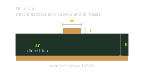
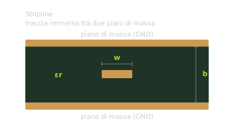
The formulae used (Wadell/IPC model, first-approximation estimate) are:
where w is the width, t the copper thickness, εr the substrate dielectric constant (≈ 4.3 for FR-4 at working frequencies, to be verified against the fabricator stack-up).
Z₀ and signal integrity
Controlled impedance exists to avoid reflections. If line, source and load are not matched, a fast edge bounces back and produces overshoot, ringing and eye degradation. The practical rule is to keep Z₀ constant along the whole path: no abrupt changes of width, reference plane or stack-up, and so on. Typical impedances are interface standards:
- 50 Ω single-ended — the default for RF, clocks and single-ended buses.
- 90 Ω differential — USB 2.0/3.x.
- 100 Ω differential — LVDS, Ethernet, PCIe, HDMI.
The tool offers two modes: forward (given the geometry, compute Z₀) and inverse design (given a target Z₀, solve by bisection for the width w that achieves it, exploiting the monotonicity of Z₀ in w). For a differential pair, start from the equivalent single-ended value: the coupling between the two traces is not modelled and must be refined on the real stack-up.
The domain of the impedance formulas
The two expressions used here are regressions, not solutions of Maxwell’s equations, and like any regression they hold over a domain. For microstrip it is 0.1 ≤ w/h ≤ 3 with 1 ≤ εr ≤ 15; outside it the error grows fast, and past a certain point the formula is not even usefully wrong any more:
| w/h | w (h = 10 mil) | Z₀ from the formula | Domain |
|---|---|---|---|
| 0.05 | 0.5 mil | 127.55 Ω | out of domain |
| 0.10 | 1.0 mil | 120.24 Ω | credited |
| 0.50 | 5.0 mil | 87.55 Ω | credited |
| 1.00 | 10.0 mil | 67.37 Ω | credited |
| 2.00 | 20.0 mil | 44.95 Ω | credited |
| 3.00 | 30.0 mil | 31.17 Ω | credited |
| 5.00 | 50.0 mil | 13.39 Ω | out of domain |
| 10.00 | 100.0 mil | −11.23 Ω | degenerate |
The bottom of the table is instructive. The logarithm’s argument is 5.98·h / (0.8·w + t), and when 0.8·w + t exceeds 5.98·h — that is around w/h = 7.3 with these values — the logarithm goes below zero and Z₀ comes out negative. That is not imprecision: it is the formula running out of domain. The tool now notices and refuses to print the number, instead of showing −11.2 Ω with the air of having computed something.
The 50 Ω geometries, and how sensitive they are
Inside the good domain the 50 Ω geometries all sit between w/h 1.4 and 2.3:
| Dielectric h | εr | w for 50 Ω | w/h |
|---|---|---|---|
| 4.0 mil | 4.3 | 5.82 mil | 1.46 |
| 6.7 mil | 4.3 | 10.93 mil | 1.63 |
| 10.0 mil | 4.3 | 17.18 mil | 1.72 |
| 10.0 mil | 3.5 | 19.17 mil | 1.92 |
| 10.0 mil | 2.2 | 23.33 mil | 2.33 |
| 20.0 mil | 4.3 | 36.11 mil | 1.81 |
The w/h ratio grows as εr falls, so a low-dielectric-constant laminate asks for wider traces for the same Z₀ — counterintuitive if one thinks of εr as something that only “slows things down”.
And the sensitivity tells you where to spend process control. Starting from w = 18 mil, h = 10 mil, εr = 4.3 (48.5 Ω):
| Deviation | Resulting Z₀ | Change |
|---|---|---|
| w +1 mil (under-etch) | 46.66 Ω | −3.71 % |
| w −1 mil | 50.35 Ω | +3.90 % |
| h +1 mil (laminate) | 51.93 Ω | +7.16 % |
| h −1 mil | 44.62 Ω | −7.92 % |
| εr +0.3 | 47.23 Ω | −2.53 % |
| εr −0.3 | 49.78 Ω | +2.74 % |
One mil of deviation on the dielectric thickness is worth twice one mil of etching, and three times a 0.3 error on εr. That is why controlled impedance is ordered from the fab as a stack-up with a declared laminate tolerance, and not as a trace width on the Gerber alone.
Limitations
- The IPC curve is empirical and derived for isolated traces: vias, adjacent planes and real densities change the heating.
- The impedance formulae are first-approximation estimates: for production layout a 2D field-solver is used, which accounts for solder mask, trapezoidal etch, copper roughness and dielectric dispersion.
- Differential coupling is not modelled; the tool reasons about a single-ended trace.
- Demonstrative tool, not an electromagnetic simulator.
References
- IPC-2221 (Generic Standard on Printed Board Design) — the standard the current–temperature-rise–cross-section curve used here comes from. Cited by name; the text is to be consulted from the IPC.
- IPC-2152 (Standard for Determining Current Carrying Capacity in Printed Board Design) — the standard dedicated to current capacity, which treats the problem as a thermal one rather than a geometric one. It is the correct reference when the sizing really matters.
- Related tool — the PCB Trace Designer puts this page into practice: give the current and get width, resistance and drop, or give the geometry (or a target Z₀) and read the controlled impedance.
A similar project?
Acoustics, embedded, calculation tools: if you have a related use case, let’s talk.