PCB Trace Designer
Size the traces of a printed circuit board: the minimum width to carry a current with a given temperature rise (IPC-2221 curve), the resistance and voltage drop; and the characteristic impedance of microstrip and stripline, with inverse design toward 50, 90 or 100 Ω. Demonstrative tool.
PCB trace designer tool
Current specification
Minimum width from the IPC-2221 curve (formerly IPC-D-275). Resistance and voltage drop use the computed width and the given length. Engineering estimation model: for production layout use a field-solver.
Result
- Cross-section area
- — mil²
- DC resistance
- —
- Voltage drop
- —
Geometry
First-approximation estimates (Wadell/IPC formulae). εr ≈ 4.3 is typical of FR-4 at working frequencies; verify against the fabricator stack-up. Differential-pair coupling is not modelled: use the equivalent single-ended value.
Result
- Topology
- —
- w / h
- —
How it works
How is trace width calculated?
A current-carrying trace heats up by Joule effect. IPC-2221 relates the DC current I to the allowed temperature rise ΔT and the copper area: A = (I / (k·ΔT^0.44))^(1/0.725), then w = A / (t·1.378). The constant k is 0.048 for external traces and 0.024 for internal ones; more copper (oz) gives a narrower trace.
A current-carrying trace heats up by Joule effect. The IPC-2221 standard (heir of IPC-D-275) relates the DC current I to the allowed temperature rise ΔT above ambient and to the copper cross-section area with an empirical law. Inverting it gives the minimum area, and dividing by the copper thickness, the width:
The constant k depends on the layer: k = 0.048 for external traces (air-cooled) and k = 0.024 for internal traces, which dissipate worse. Halving k does not double the width: the exponent is 1/0.725, so the factor is 21/0.725 ≈ 2.6. Thickness is measured in ounces (oz): 1 oz ≈ 35 µm ≈ 1.378 mil of copper; more copper = a narrower trace for the same current.
Why do ΔT and derating matter?
ΔT is the design choice: 10 °C is conservative, 20–30 °C is common in consumer electronics, but it adds to the ambient temperature and to that of nearby components. The IPC curve holds for isolated traces in still air; on a dense board the real heating is worse, so a derating is applied by choosing a lower ΔT and leaving margin.
ΔT is not a detail: it is the design choice. A ΔT of 10 °C is conservative, 20–30 °C is common in consumer electronics, but it adds to the maximum ambient temperature and to that of nearby components. The IPC curve is derived for isolated traces in still air: on a dense board, near heat sources or with little surrounding copper, the real heating is worse. That is why a derating is applied — a ΔT lower than the limit is chosen — leaving margin. DC resistance and voltage drop follow from the copper resistivity:
with ρ₂₀ ≈ 1.724·10⁻⁸ Ω·m and α ≈ 0.00393 /°C: copper is a PTC conductor, its resistance rises with temperature. A seemingly small voltage drop on a supply rail can matter on a low-voltage distribution.
What are microstrip and stripline?
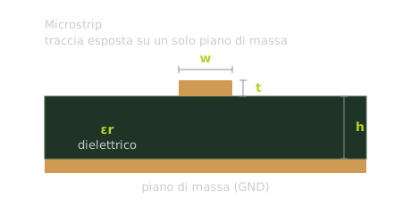
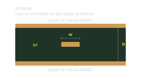
At high frequency a trace is a transmission line with its own characteristic impedance Z₀, set by geometry and dielectric. A microstrip runs on an outer layer with a single ground plane below: simpler, but part of the field travels in air. A stripline is buried between two planes: field entirely in the dielectric, better shielding, but narrower for the same Z₀.
When the signal goes high in frequency (fast clocks, serial buses, RF), a trace is no longer a plain wire: it is a transmission line with its own characteristic impedance Z₀, set by the geometry and the dielectric. The two most common topologies:
- Microstrip — a trace on an outer layer with a single ground plane below, separated by a dielectric of height h. Simpler to fabricate, but part of the field travels in air (lower effective εr) and it is exposed to emissions.
- Stripline — a trace buried in an inner layer between two ground planes spaced b apart. Field entirely in the dielectric, better shielding and lower crosstalk, at the cost of a narrower trace for the same Z₀ and a more complex stack-up.
Why is controlled impedance needed?
Controlled impedance avoids reflections: if line, source and load are not matched, a fast edge bounces back creating overshoot, ringing and eye degradation. The rule is to keep Z₀ constant along the whole path, with no abrupt changes of width or reference plane. Typical values: 50 Ω single-ended, 90 Ω differential (USB), 100 Ω differential (LVDS, Ethernet, PCIe, HDMI).
Controlled impedance exists to avoid reflections: if line, source and load are not matched, a fast edge bounces back creating overshoot, ringing and eye degradation. The rule is to keep Z₀ constant along the whole path — no abrupt changes of width, reference plane or stack-up. Typical impedances are interface standards:
- 50 Ω single-ended — the default for RF, clocks and single-ended buses.
- 90 Ω differential — USB 2.0/3.x.
- 100 Ω differential — LVDS, Ethernet, PCIe, HDMI.
Inverse design fixes the dielectric and copper thickness and solves by bisection for the width w that yields the target impedance (Z₀ is monotonically decreasing in w). For a differential pair, start from the equivalent single-ended value and refine on the fabricator real stack-up.
Engineering estimates per the IPC-2221 model; not a substitute for a 2D field-solver.